xSPI

Overview
Emerging high-performance applications demand increasingly fast read
throughputs from NOR_Flash/ NAND Flash/ HyperRAM memory devices As new age lower-end microcontrollers (MCUs) continue to shrink in die size, their internal memory is very limited. They need a low pin count,
high-performance memory subsystem. Similarly, there are consumer
applications that are space-constrained and require instant-on, such
as digital still cameras, DSLRs and home automation. So, OEMs are
looking for simple, flexible, high performance and low-energy memory
solutions with backward compatibility to meet their needs. The major
NOR Flash memory device vendors responded with such devices by
expanding from current Quad I/O to OctaFlash Memory (8 I/O) resulted
in substantial increase in Serial NOR Flash throughput.
For example, the new-generation OctaFlash by Macronix is built on
Serial Peripheral Interface (SPI) and command set, providing extendable
I/O capability(x8). The data transfer rate has been increased from
100MB/s of Quad I/O Serial NOR Flash to 400MB/s, claims Macronix.
This resulted in lower-density memory subsystem interfaces trending
toward x4/x8 SPI (xSPI) interfaces and performance growing
exponentially. Mobiveil’s approach on this emerging scenario results in
adapting to JEDEC xSPI compliant NOR Flash/ NAND Flash controller
supporting devices from various vendors. The IP can function as
simple ‘SPI Flash Controller’ or, ‘Quad-SPI Flash Controller or Octa-
SPI Flash Controller’ or ‘Dual QSPI Controller’, thus compatible with
legacy devices also. The controller architecture is SoC friendly and
supports multiple chip-selects.
- Winbond Octal NAND W35N04JWXXIC
- Winbond NAND W25N01GWxxIG
- Winbond NOR W25Q512JVxIQ
- Adesto AT25XP032
- Micron MT35XL256ABA
- Micron MT25QU01GBBB8E0 (x4)
- Macronix MX25UM51245G
- Cypress HyperFlash S26KL512S
- Cypress Semper S26HS01GT
- Supports Cypress Hyperram S27KL0643
- All similar devices in Market
- Complaint to JESD251A Specification
- Memory mapped access to the connected flash devices
- Continuous Burst transfer support
- Auto boot support
- XIP support
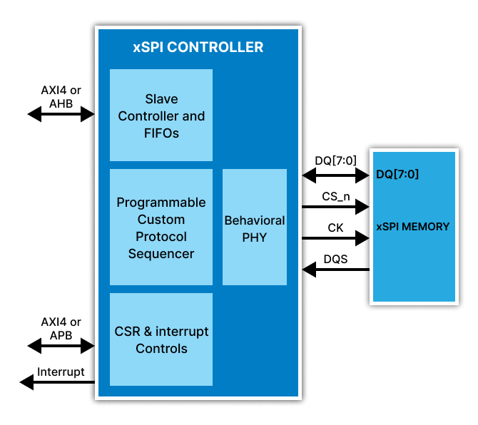
- AXI4 or AHB-Lite system interface for memory access with outstanding address support
- AXI4 or APB interface port for CSR register access
- Custom protocol Sequence based design to support an array of vendors

Design Attributes
• Highly modular and programmable design • Fully synchronous design • Software control for key featuresProduct Package
• RTL Code • System Verilog/UVM based Testbench • Test cases • Protocol checkers and bus watchersDocumentation
• Design Guide • Verification Guide • Synthesis GuideLicensing Options
• Single Design or Multi-project license (HDL Source Code)Get the Detailed Product Brief here

