ONFI/Toggle IP

Overview
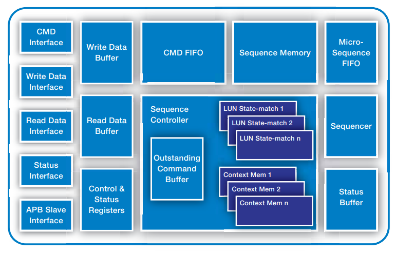
Mobiveil’s ONFI/Toggle IP is a highly flexible and configurable design targeted for enterprise storage applications like SSD. The ONFI/Toggle IP is used to access the external NAND flash for high speed transactions of multiple pages of read or write data taking advantage of the pipeline performance of newer enterprise NAND flash devices. The controller architecture allows control of most all ONFI 5.2 and toggle devices with flexible addressing schemes.
NAND Flash
- Supports ONFI 5.2 all modes
- Supports Toggle mode NAND interface
- LDPC error correction available
- Data path widths support of 16 bits to 256 bits PHY Data path width - 16 bit , 32bit
- Supports ONFI 5.2 specification with NV-LPDDR4 mode of operation
- Device independent RTL can work with any NAND device with just software reprogramming
- Configurable Ready Busy Signal Configuration (Per device or Wired OR)
- Supports volume addressing, suspend/resume functions, two pass programming, multi plane and asynchronous plane read commands
- Supports User Interface to be Asynchronous with Flash Interface
- Supports upto 256 LUNs per channel
- Supports virtual LUNs feature to limit the gate count of EFC based on maximum possible simultaneous LUN operations in the end user system
- Configurable warmup cycles through CSR register
- DBI support


NAND Flash Control Processor
• Create any kind of flash control sequences that are needed in your environment • Command can be created to be run in parallel with or without data and run in different LUN's or chip selects • Transaction based user interface • Software definable address schemeDesign Attributes
• Highly modular and configurable design • Fully synchronous design • Totally software configurable at runtimeProduct Package
• Configurable RTL Code • HVL based test bench & Test cases • Design, Verification & Synthesis Guide • FPGA Netlist for Prototype • Synthesis Scripts • DocumentationGet the Detailed Product Brief here
OCTA PSRAM

