HyperBus

Overview
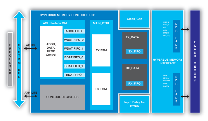
Mobiveil’s HyperBus flash Interface is a low pin count interface that achieves significantly higher performance than legacy parallel and SPI interfaces for SPI based NOR flashes. This controller Interface involves a simple read/write protocol that is suitable for both memories and peripheral interfaces. Interestingly, this interface only requires an additional six pins more than the QSPI. The HyperFlash memories coupled with our Hyperbus flash controller provide a new standard for performance by delivering upto 333 MB/s using this 12-pin interface.
- Compatible with Cypress/Spansion hyperbus based memory products
- 0 Wait State Write Burst Operation for HyperBus memory on AXI interface of up to 256 words
- True Continuous Burst Read operation for HyperFlash on HyperBus memory interface
- AXI-lite port for control registers accesses
- Minimum Gap between two Read Operations for highest performance on HyperBus memory interface
- Cache Line accesses for Execution-in-Place (XiP)
- HyperBus memory device clock of up to 166MHz. Up to 16 outstanding address support in AXI
- Compatible with spansion hyperbus based memory products
- 0 Wait State Write Burst Operation for HyperBus memory on AXI interface of upto 256 words
- AXI-lite port for control registers accesses
- True Continuous Burst Read operation for HyperFlash on HyperBus memory interface
- Minimum Gap between two Read Operations for highest performance on HyperBus memory interface
- Cache Line accesses for Execution-in-Place (XiP)
- HyperBus memory device clock of upto 166MHz
- Upto 16 outstanding address support in AXI

Configurable Options
• Internal FIFO Depths is configurable • AXI parameters configurableDesign Attributes
• Highly modular design • Clearly demarked clock domains • Software control for key features • Loopback for DebuggingProduct Package
• Configurable RTL Code • HDL based test bench and behavioral models • Test cases • Protocol checkers, bus watchers and performance monitorsDocumentation
• Design Guide • Verification Guide • Application NoteGet the Detailed Product Brief here
OCTA PSRAM

